

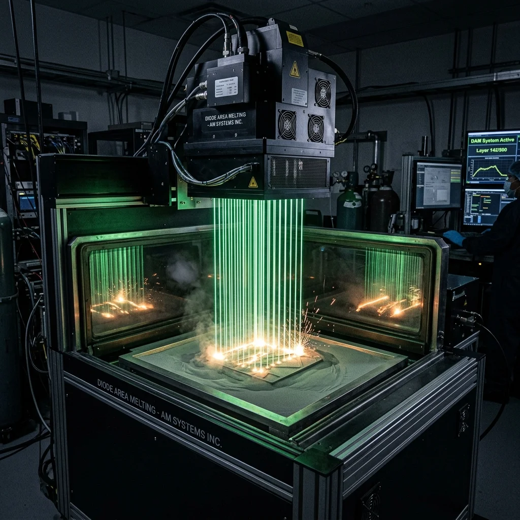
In 2025–2026, Diode Area Melting (DAM) reimagines metal PBF by replacing sequential laser scanning with a massively parallel array of diode lasers that illuminate entire zones simultaneously: conceptually a “DLP projector for metal powder.”
Principle: Area Melting vs. Point Scanning
| Parameter | Conventional PBF (Laser) | DAM (Diode Array) |
|---|---|---|
| Source | 1–12 point lasers | Array of 10,000+ diodes |
| Mode | Sequential scanning | Parallel area irradiation |
| Power | 200–1000W/laser | 1–5W/diode × 1000 = kW total |
| Layer Time | Minutes | Seconds |
| Pixel | Laser spot ~80 μm | Diode pixel ~100–200 μm |
Interactive Filament Selector
Answer 3 quick questions and find the optimal material for your project.
1. What are the mechanical requirements for the part?
2. What temperature will the part operate at?
3. Are there any specific environmental requirements?
Our recommendation:
PLA filament
Ideal for easy printing, model visualization and decorative parts.
Pros and Cons
Pros:
- Massive Parallelism: 10,000+ laser points operating simultaneously.
- Homogeneous Thermal Field: No “hot” and “cold” zones from serpentine scanning.
- Potentially Lower Cost: Diode lasers are significantly cheaper than fiber lasers.
- Scalability: Adding more diodes increases build area without speed loss.
Cons:
- Lower Resolution: Diode pixels larger than fiber laser spot.
- Immature Technology: Few commercial systems (Seurat Technologies is the leader).
- Thermal Control: Managing 10,000+ individual diodes is a software challenge.
FAQ
Diode Area Melting (Dam): Massive Parallelism In Metal Pbf Calculator
Interactive optimization calculator.
The full picture
This article is one page from The Big Book of 3D Printing: 704 illustrated pages covering every technology, material and fix in one reference.
Read it on Kindle →Engineer, author of The Big Book of 3D Printing and additive manufacturing expert