

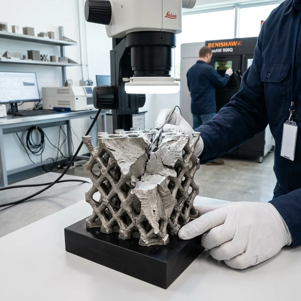
Additive manufacturing (AM) has transitioned from rapid prototyping to producing mission-critical end-use parts. However, the complex thermal dynamics, layer-by-layer material deposition, and intricate metallurgical interactions inherent to 3D printing introduce unique failure mechanisms. Identifying the root cause of a failed AM component is no longer just about visual inspection; it requires a sophisticated forensic approach.
Failure analysis in additive manufacturing is the critical bridge between experimental design and industrial reliability, ensuring that every printed part meets the stringent demands of aerospace, medical, and automotive applications. In this deep dive, we will explore the methods engineers use to dissect, diagnose, and prevent failures in 3D-printed components. From non-destructive in-situ monitoring to microstructural analysis at the crystallographic level, mastering these tools is essential for any modern manufacturing engineer.
Non-Destructive Testing (NDT): Seeing Inside the Solid
Before a failed part is sectioned or altered, non-destructive testing (NDT) provides the first glimpse into its internal architecture. X-ray Computed Tomography (Micro-CT) is the gold standard here, allowing engineers to visualize internal defects in 3D without compromising the specimen. Micro-CT can accurately map porosity, lack of fusion (LoF) defects, and trapped un-melted powder. Beyond static imaging, Digital Image Correlation (DIC) is increasingly used during mechanical testing to measure surface strain and displacement in real-time. By tracking how a part deforms under load, DIC highlights stress concentrations that often serve as the nucleation sites for cracks, providing a macroscopic map of potential failure points before they fully manifest.
In-Situ Monitoring and Acoustic Emission (AE)
The ultimate goal of failure analysis is to move from post-mortem investigation to real-time prevention. Acoustic Emission (AE) represents a leap forward in this domain. AE is a passive NDE technique that detects transient elastic waves generated by rapid energy releases within the material: such as crack initiation, propagation, or layer delamination. By integrating AE sensors directly into the printer or the testing rig, engineers can pinpoint the exact moment and location of a microscopic failure as it happens. This real-time damage monitoring allows for the classification of different failure modes based on signal frequency and amplitude, providing a dynamic understanding of structural integrity that static post-print analysis simply cannot offer.
Microstructural Forensics: SEM and EBSD
To understand *why* a failure occurred, analysts must look at the microstructural context. Scanning Electron Microscopy (SEM) is indispensable for fractography, enabling the high-magnification examination of fracture surfaces to determine whether a failure was ductile, brittle, or fatigue-driven. However, when combined with Electron Backscatter Diffraction (EBSD), the analysis reaches a new dimension. EBSD maps crystallographic orientation, grain size, phase distribution, and local strain. By applying EBSD to a fracture cross-section, engineers can correlate failure sites with specific microstructural anomalies, such as detrimental phase transformations (e.g., in Titanium alloys) or residual strain regions. This level of detail is crucial for linking material science directly to printer process parameters.
The Digital Thread and Predictive Modeling
Modern failure analysis is highly data-driven. The concept of the "Digital Thread" involves maintaining a complete, traceable record of a part's lifecycle, from raw powder characteristics (using techniques like helium pycnometry and powder rheology) to specific laser paths and ambient build conditions. When a part fails, engineers can trace the defect back to a precise anomaly in the build logs. Furthermore, the synthesis of experimental data from AE and microstructural maps from EBSD is increasingly being used to feed Finite Element Analysis (FEA) and Machine Learning models. This synergistic approach allows manufacturers to transition from reactive troubleshooting to predictive modeling, optimizing scan strategies and cooling rates to proactively eliminate the physical conditions that lead to failure.
Conclusion
Failure analysis in additive manufacturing is a multi-disciplinary science that merges material characterization, real-time sensor data, and advanced computational modeling. By leveraging methods like Micro-CT, Acoustic Emission, and EBSD, engineers can decode the complex forensic history of any 3D-printed part. As we continue to push the boundaries of what AM can achieve, mastering these diagnostic tools will be the key to unlocking zero-defect manufacturing and absolute structural confidence.
The full picture
This article is one page from The Big Book of 3D Printing: 704 illustrated pages covering every technology, material and fix in one reference.
Read it on Kindle →Engineer, author of The Big Book of 3D Printing and additive manufacturing expert