

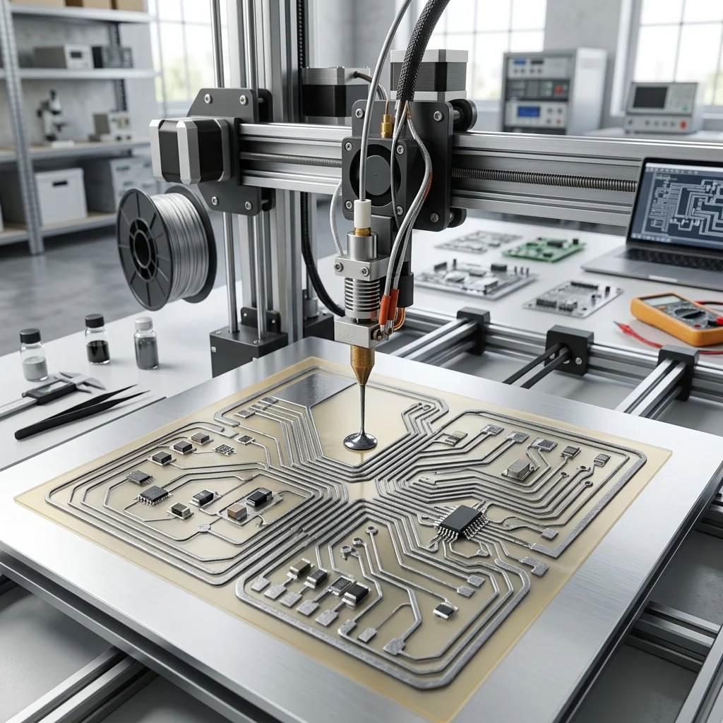
3D printing has long outgrown its original role as a mere structural prototyping tool. Today, we are entering the era of genuine 3D mechatronics: a new engineering paradigm where the physical form and functional electronic circuitry are manufactured simultaneously and monolithically. At the core of this revolution is conductive ink 3D printing.
By overcoming the geometric limitations of rigid, two-dimensional printed circuit boards (PCBs) and transitioning toward flexible, conformal 3D electronics, we are fundamentally redefining the anatomy of smart devices. From aerospace components featuring embedded antennas to intelligent, biocompatible prostheses capable of registering touch, the ability to extrude or atomize electrical pathways onto arbitrary geometries provides unprecedented freedom in hardware design.
The Chemistry and Rheology of Conductive Inks
The magic of 3D printed electronics begins at the molecular level. Conductive inks are not simply 'liquid wires.' They are highly engineered suspensions comprising three main components: conductive fillers (typically silver, copper, or carbon nanoparticles and flakes), a polymeric binder for structural adhesion, and a vehicle solvent that dictates flow characteristics. The rheology of these inks must be meticulously calibrated: they need to flow smoothly under shear stress through a microscopic nozzle, yet instantly recover their structural integrity upon deposition to prevent unwanted spreading. While copper nanoparticles offer a cost-effective alternative to silver, they demand complex encapsulation strategies to prevent oxidation during the printing and curing phases.
Advanced Sintering: From Liquid to Crystalline Network
Immediately after deposition, the printed 'wire' is usually poorly conductive. To establish a continuous electrical pathway, it must undergo a sintering process. Conventional thermal sintering in an oven is effective but risks damaging the underlying substrate, particularly when printing on temperature-sensitive polymers like PLA or PETG. This is where advanced manufacturing techniques excel: photonic sintering using xenon flash lamps, microwave heating, as well as laser and chemical sintering. These innovations deliver concentrated, localized energy to the ink in a matter of milliseconds, melting the nanoparticles into a dense, highly conductive network without deforming the plastic foundation.
Manufacturing Processes: DIW vs. Aerosol Jet Printing
When it comes to depositing these specialized materials, the industry relies heavily on two technologies. Direct Ink Writing (DIW) is an extrusion-based process where highly viscous pastes are pneumatically or mechanically pushed through a micro-nozzle. It is exceptionally versatile and supports the fabrication of complex, high-aspect-ratio structures. Conversely, Aerosol Jet Printing (AJP) is a non-contact method that atomizes the ink into a fine mist, which is then dynamically focused by a sheath gas onto the substrate. AJP achieves astonishing resolution (often down to 10–20 micrometers) making it the undisputed champion for printing ultra-fine interconnects over complex, non-planar 3D topologies.
Conformal Electronics: The End of the Green Board
Traditional PCB manufacturing relies on a subtractive process burdened with chemical etching, toxic waste, and strict 2D planar constraints. Additively Manufactured Electronics (AME) enable 'conformal' printing, where the circuitry adapts to the shape of the object rather than forcing the object to accommodate the board. Imagine a drone whose structural wings simultaneously act as antennas and environmental sensors, thanks to embedded silver traces. Or a smart ring where the battery matrix and logic pathways are directly printed into the structural polymer resin. This convergence of form and function not only saves critical space and weight but also dramatically reduces e-waste.
Conclusion
The 3D printing of electronics is entirely rewriting the rulebook of hardware design. By mastering conductive inks and deposition technologies like DIW and Aerosol Jet, we are no longer building hollow enclosures to hide messy wiring: we are transforming the product itself into a fully integrated, functional electronic system. The future of personalized mechatronics is unfolding right now, and we have only just scratched the surface.
The full picture
This article is one page from The Big Book of 3D Printing: 704 illustrated pages covering every technology, material and fix in one reference.
Read it on Kindle →Engineer, author of The Big Book of 3D Printing and additive manufacturing expert